Quantum computers are expected to vastly outperform conventional computers in tackling highly complex computational challenges, including drug discovery and the simulation of advanced physical systems. However, building a practical quantum computer will require millions of interconnected qubits that can operate with high precision and reliability.
Among the many quantum computing approaches currently being explored, silicon quantum dot spin qubits are regarded as one of the strongest candidates for large-scale industrial manufacturing, often earning the label of “industry qubits”. Their fabrication process is highly compatible with conventional silicon chip production based on CMOS technology — an area in which imec has established extensive expertise over several decades.
“We are able to build upon decades of semiconductor innovation and make use of the existing silicon manufacturing ecosystem, enabling quantum devices to move beyond laboratory experiments towards scalable and manufacturable systems. This is where silicon-based qubits offer a distinct advantage,” said Sofie Beyne, project leader and quantum integration engineer at imec.
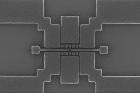
Silicon quantum dot spin qubits operate by trapping an electron inside a silicon nanostructure known as the gate layer. The spin state of the electron is then used to store quantum information. To minimise environmental noise, the spacing between the gates must be extremely small. Imec has now demonstrated a functioning qubit network with gaps measuring only six nanometres. At this scale, it is theoretically possible to integrate millions of qubits onto a single chip.
“High NA EUV makes it possible to precisely pattern silicon quantum dot qubits. Since the coupling strength between neighbouring quantum dots increases exponentially as the gap narrows, we need to reliably create electrode gaps measuring only a few nanometres. Achieving this is a remarkable engineering accomplishment, made possible by the efforts of our integration and patterning teams together with ASML’s advanced High NA EUV technology,” said Kristiaan De Greve, imec fellow and programme director for quantum computing.
The latest demonstration builds on imec’s earlier work involving silicon quantum dot spin qubits, which had already shown that CMOS-compatible manufacturing processes could deliver stable qubit performance with low charge noise. By incorporating High NA EUV lithography into the fabrication process, the focus is now shifting from isolated laboratory prototypes towards reproducible quantum devices compatible with 300mm semiconductor fabrication facilities.
While High NA EUV lithography is already considered essential for sub-2nm logic chips and high-density memory technologies supporting the rapid expansion of AI and high-performance computing, the technology is now also emerging as a potentially critical enabler for next-generation quantum computing hardware.