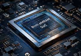
SEMIFIVE and ICY Tech Achieve 8nm eMRAM Edge AI SoC Tape-Out with Samsung Foundry
The successful tape-out of a next-generation Edge AI SoC using Samsung Foundry’s 8nm eMRAM technology positions SEMIFIVE and ICY Tech at the forefront of ultra-low-power AI inference, advancing commercial deployment of MRAM-based edge semiconductors for robotics, AI PCs, automotive, and offline AI applications.
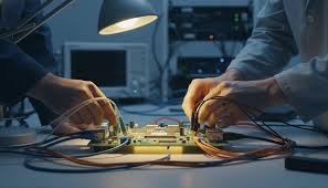
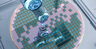
SEMIFIVE, a leading global provider of custom AI semiconductor (ASIC) solutions, and ICY Tech, a Chinese AI semiconductor company, announced the successful tape-out of next-generation Edge AI SoC jointly developed utilising Samsung Foundry's 8nm (8LPU) embedded Magnetic Random Access Memory (eMRAM) technology. This marks a significant milestone toward the first commercial deployment of 8nm eMRAM technology in Asia.
This collaboration represents SEMIFIVE's first ASIC design project leveraging eMRAM technology. By integrating eMRAM into an Edge AI accelerator, the company aims to reinforce its technical leadership in the ultra-low-power, high-performance inference market.
Compared to SRAM, eMRAM features a smaller bit cell, enabling higher data density within the same area. Unlike DRAM, it does not require periodic refresh operations, significantly reducing power consumption. With its non-volatile characteristics that retain data even when power is removed, eMRAM is widely regarded as a "universal memory" particularly well-suited for environments with power and area constraints, such as edge devices.
Originating from the Applied Magnetism Centre of the School of Physics at Peking University, ICY Tech brings deep insight and extensive experience in magnetism and spintronics, enabling highly customised MRAM development tailored for AI inference scenarios. This includes MRAM bit-cell and peripheral circuits, as well as globally leading and uniquely patented accelerator designs for high-bandwidth readout and in-situ matrix-vector multiplication (GEMV).
SEMIFIVE is a key Design Solution Partner (DSP) in the Samsung Foundry SAFE™ ecosystem and a global AI ASIC specialist with a proven track record of successfully delivering advanced custom semiconductor projects ranging from AI/HPC to Edge AI. The company provides comprehensive engineering services from spec consulting to mass production, serving a broad range of customers, including fabless companies, service providers, and system OEMs.
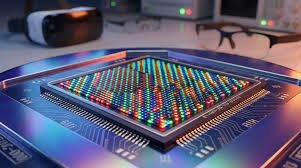
For this project, SEMIFIVE provided comprehensive ASIC design services and transformed ICY Tech's novel architecture into production-ready silicon. By integrating ICY Tech's Processing Near Memory (PNM) technology with SEMIFIVE's proprietary SoC design platform, the two companies developed an optimised architecture capable of high-speed, on-device inference for models with up to 2B parameters in edge environments. This enables operation without any network connectivity. At the 2B-parameter scale, practical AI tasks such as text summarisation, translation, and conversational inference become feasible on-device. This capability has been challenging to achieve with conventional SRAM-based edge AI chips due to physical limitations in die area and power.
This architecture is designed for edge devices operating in offline environments, including AI PCs, private AI agents, and humanoid robots. Target applications encompass robotics (physical AI), automotive semiconductors (such as autonomous driving and digital cockpits), and smart devices.
"This collaboration is a highly challenging project to bring a spintronics-based AI inference architecture into silicon using Samsung Foundry's 8nm (8LPU) process. By fully integrating the non-volatile and ultra-low-power characteristics of eMRAM into AI accelerators, we believe this will set a new milestone for edge AI semiconductors," said Yves Zhu, CEO of ICY Tech. "With SEMIFIVE's proven comprehensive ASIC design capabilities, ICY Tech's unique customisation capabilities in MRAM bit-cell peripheral circuits, and Samsung Foundry's advanced eMRAM process, we are confident this project will establish a new standard for performance and power efficiency that surpasses the limitations of existing architectures in the global AI inference market."
"In the AI era, semiconductors are rapidly shifting from off-the-shelf components to custom-built solutions tailored to specific needs. As the Edge AI market expands, the architectures requested by customers are becoming increasingly sophisticated and diverse," said Brandon Cho, CEO and co-founder of SEMIFIVE. "As ASIC design involving next-generation memories like eMRAM gains momentum, the role of a specialised partner managing the entire process becomes vital. As a key partner in the Samsung Foundry SAFE™ ecosystem, SEMIFIVE has successfully executed numerous AI, HPC, and Edge AI projects. Through our partnership with ICY Tech, we are proud to expand our portfolio into the emerging domain of MRAM-based design."
MRAM/eMRAM
Magnetic Random Access Memory (MRAM) is a next-generation memory technology that utilises Magnetic Tunnel Junction (MTJ) elements. It combines the non-volatile characteristics of NAND Flash, retaining data even when power is removed, with high-speed performance comparable to DRAM. With write speeds over 1,000 times faster than flash memory and significantly lower power consumption, MRAM is emerging as a core technology for AI semiconductors and low-power edge devices. In particular, embedded MRAM (eMRAM) refers to MRAM technology integrated directly into system semiconductors such as SoCs and MCUs. It is widely regarded as a next-generation on-chip memory solution to replace conventional embedded Flash (eFlash).
Unlike traditional DRAM, MRAM is a type of resistive memory. While DRAM is based on electrical charge storage, MRAM relies on the resistance changes within the MTJ unit cell. DRAM has achieved significant advancements in density, bandwidth, and power efficiency. However, it requires continuous refresh operations to retain data, consuming standby power even when not actively in use. In contrast, MRAM can preserve data for extended periods without refreshing operations. For this reason, it is gaining attention as a "universal memory" with the potential to fundamentally transform current computing architectures.