Keysight Technologies Launches Semiconductor Lab Solutions to Bridge Skills Gap
New teaching platforms deliver hands-on training aligned with real-world R&D and manufacturing workflows
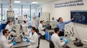
Keysight Technologies, Inc. (NYSE: KEYS) announced three new semiconductor teaching lab solutions designed to help universities prepare students for careers in the global semiconductor industry. The three solutions—Basic Design and Measurement, Parametric Test and On-Wafer Measurement, and Photonics IC Measurement—provide students with practical experience using professional-grade tools and workflows that are commonly used in semiconductor research, development, and manufacturing.
As the semiconductor industry accelerates globally, universities face increasing pressure to produce graduates who are industry‑ready. Academic institutions recognise that theory alone is no longer sufficient, and students must gain hands‑on experience with the same measurement techniques, workflows, and tools used in real semiconductor R&D and manufacturing environments.
Keysight addresses this challenge by providing solutions designed for training and development. As part of this effort, Keysight delivers a structured, progressive learning pathway that mirrors real-world semiconductor test workflows. Students gain hands-on experience setting up professional measurement hardware, performing fundamental electrical tests, device characterisation, and photonic IC characterisation using industry-standard equipment with guided lab modules.
Key benefits include:
- Hands-on training with industry-standard semiconductor instruments, measurements, and workflows.
- Structured lab modules that help students connect textbook concepts to real-world semiconductor applications.
- A learning approach that aligns theory with practice and prepares students for professional engineering careers.
Lim Han Sing, Vice President, General Electronics Measurement Solutions at Keysight Technologies, said: “Both educators and the wider industry play a critical role in developing the next generation of semiconductor engineers. By bringing real-world measurement techniques into the classroom, Keysight is helping educators deliver practical, job-relevant training that aligns closely with industry needs. This move will bridge the gap between education and practical experience, supporting the future workforce.”
Resources