Rigaku Corporation Expands Semiconductor Metrology R&D Through Strategic Collaboration with imec
Three-year development program targets next-generation AI semiconductor inspection technologies for CFET, EUV lithography, advanced packaging, and 3D memory applications.
Rigaku Corporation, a global solution partner in X-ray analytical systems and a group company of Rigaku Holdings Corporation (headquarters: Akishima, Tokyo; CEO: Jun Kawakami; “Rigaku”), announced the expansion of its metrology technology development for next-generation semiconductors, leveraging global research environments.
As part of this initiative, Rigaku is working with imec, a world-leading semiconductor research and innovation hub headquartered in Belgium, under a three-year development program. Through this effort, Rigaku will advance its core X-ray technologies, including 3D device metrology, high-sensitivity detection of ultrathin films and trace elements, and non-destructive inspection of microscopic defects.
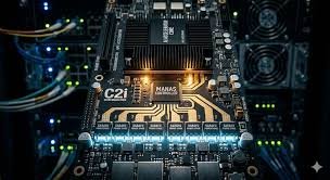
As semiconductor devices evolve toward advanced architectures such as Gate-All-Around (GAA) and Complementary FET (CFET)1, and memory density increases, manufacturing processes are becoming more complex. These drives are growing demand for highly accurate, non-destructive measurement and inspection technologies to support stable mass production. Rigaku addresses these needs by delivering high-value, differentiated metrology and inspection solutions.
Key focus areas
- Advanced logic: Metrology and inspection technologies for CFET devices
- Reticle metrology: Evaluation of photomask degradation used in EUV2 lithography
- Advanced wiring and packaging 3: Non-destructive inspection technologies
- Advanced memory: Evaluation of nanostructures in 3D DRAM (a next-generation memory device)
Markus Kuhn, Executive Officer and General Manager of Semiconductor Metrology Division of Rigaku, commented, “The serviceable available market (SAM) for Rigaku’s metrology and inspection products in the advanced AI semiconductors is expected to reach approximately US$1 billion by 2030. To address this market growth, Rigaku will continue introducing high‑value, differentiated products, to achieve a 50% share of this SAM. Strengthening our collaboration with imec will further enhance our competitiveness in high-value-added measurement and inspection, supporting medium- to long-term growth.”
1 GAA/CFET: Gate-All-Around / Complementary Field-Effect Transistors. A next-generation device architecture in which n-type and p-type transistors are vertically stacked to increase device density beyond nanosheet (GAA) technology.
2 EUV exposure: A core technology for advanced semiconductor manufacturing that enables the formation of ultrafine circuit patterns.
3 Advanced packaging: Packaging technologies that integrate multiple semiconductor chips to enhance performance and reduce power consumption