ZEISS Opens First Semiconductor Innovation Centre in South Korea
The new research facility in Yongin brings semiconductor development closer to customers, supporting advanced packaging, EUV lithography and next-generation chip manufacturing technologies.
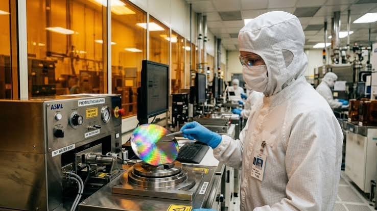
German optics and technology company ZEISS has opened its first Semiconductor Innovation Centre in Yongin, South Korea, bringing its research and development capabilities closer to customers' semiconductor manufacturing facilities. The new centre is designed to accelerate the development of advanced semiconductor manufacturing technologies, particularly for extreme ultraviolet lithography and next-generation packaging processes.
Speaking during the opening of the ZEISS Korea Yongin Semiconductor Innovation Centre, Matthew Wilson, Vice President and Head of the Semiconductor Manufacturing Technology Business at ZEISS Korea, said the facility was established to give Korean customers faster access to the company's technology and engineering expertise.
Located within SurplusGLOBAL's Yongin Semiconductor Equipment Cluster, the approximately 350-square-metre facility can accommodate up to four semiconductor manufacturing systems simultaneously. ZEISS said the centre will support the continuous advancement of semiconductor manufacturing equipment while aligning with customers' long-term technology roadmaps. The company also plans to invest further in expanding the site's capabilities over the next decade.
Previously, Korean semiconductor manufacturers were required to send wafers and photomask samples to ZEISS research facilities in Germany, the United States or Israel for equipment evaluation. The company said establishing a local research centre will eliminate logistical delays, simplify collaboration and accelerate the commercialisation of new semiconductor manufacturing technologies.
ZEISS selected South Korea for its first Semiconductor Innovation Centre for several strategic reasons. The company highlighted the country's leadership in artificial intelligence semiconductors, advanced packaging and next-generation memory technologies. ZEISS also has an established presence in Seoul and Dongtan, supported by more than 100 Semiconductor Manufacturing Technology engineers, enabling close collaboration with local customers. In addition, carrying out research activities locally reduces international transportation requirements, contributing to the company's sustainability objectives by lowering carbon emissions.
The innovation centre will serve as a collaborative research facility where customers can evaluate the latest ZEISS semiconductor equipment through demonstration programmes and Joint Evaluation Programmes. Customer feedback collected during these evaluations will be incorporated into future product development, allowing the company to refine and customise equipment for specific manufacturing requirements.
Michael Henschel, Head of Advanced Packaging at ZEISS, said research findings generated through customer collaborations will be shared with the company's headquarters in Germany, enabling faster development of semiconductor manufacturing technologies tailored to market needs. Once the equipment reaches commercial readiness, it can be transferred directly into customers' production facilities.
The centre currently houses two advanced semiconductor systems: the ZEISS NLX-100 and the DUNE 100.
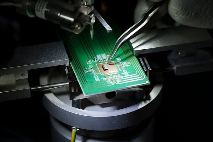
The NLX-100 is a metrology and inspection platform designed for advanced semiconductor packaging. Using automated inline three-dimensional X-ray laminography for 300 mm wafers, the system enables non-destructive inspection of complex internal structures such as stacked dies, micro-bumps and through-silicon vias. ZEISS said the solution combines high-speed inspection with high-resolution imaging and integrates in-house developed X-ray technology with its artificial intelligence-powered ZEISS INSPECT software for data analysis.
According to Henschel, as semiconductor packaging technologies such as hybrid copper bonding continue to evolve, achieving higher X-ray resolution without damaging devices has become increasingly important. The NLX-100 was engineered to precisely control radiation exposure while maintaining imaging performance.
The second system, DUNE 100, is designed to measure and correct wafer warpage during semiconductor manufacturing. The equipment can flatten both complete wafers and selected regions in a single processing step without requiring chemical materials typically used in conventional polishing processes. ZEISS said the technology helps improve manufacturing precision while reducing process complexity.
Karoline Pigdon, Head of Semiconductor Fab Solutions at ZEISS, described the DUNE 100 as an important inline manufacturing solution capable of improving production yields, particularly during wafer bonding processes where wafer warpage can significantly affect manufacturing performance.
Later this year, ZEISS also plans to install a prototype of its MERIT AE photomask repair system at the Yongin facility. The system has been developed for repairing microscopic defects in photomasks used in high numerical aperture extreme ultraviolet lithography and offers enhanced repair capabilities compared with the company's previous generation technology.
ZEISS said the Yongin Semiconductor Innovation Centre will continue to expand with additional semiconductor technologies and equipment as it strengthens collaboration with chip manufacturers and supports the industry's transition towards increasingly advanced semiconductor production.