EUV Lithography Market Set for Strong Growth Through 2032
Rising demand from AI, high-performance computing, and advanced semiconductor manufacturing drives market expansion
According to MarketsandMarkets™, the Extreme Ultraviolet (EUV) Lithography Market is projected to grow from USD 15.84 billion in 2026 to USD 30.36 billion by 2032, at a CAGR of 11.4%.
Browse 116 market data Tables and 68 Figures spread through 206 Pages and an in-depth TOC on "Extreme Ultraviolet (EUV) Lithography Market - Global Forecast to 2032"
Extreme Ultraviolet (EUV) Lithography Market Size & Forecast:
- Market Size Available for Years: 2021–2032
- 2026 Market Size: USD 15.84 billion
- 2032 Projected Market Size: USD 30.36 billion
- CAGR (2026–2032): 11.4%
Extreme Ultraviolet (EUV) Lithography Market Trends & Insights:
- The extreme ultraviolet (EUV) lithography market is driven by the adoption of data-driven technologies, artificial intelligence (AI), and high-performance computing (HPC) applications, which in turn drive demand for more advanced and efficient semiconductor solutions. As industries increasingly rely on data analytics, AI, and machine learning (ML) to enhance decision-making and operational efficiency, demand for high-density, high-performance integrated circuits (ICs) is growing.
- By component, light sources accounted for the largest market share of 53.4% in 2025.
- By system type, 0.55 NA EUV systems are expected to register the highest CAGR of 28.0% during the forecast period.
- By end user, foundries are expected to record a significant CAGR in the extreme ultraviolet (EUV) lithography market during the forecast period.
- By region, the Asia Pacific region accounted for 85.8% market share in 2025.
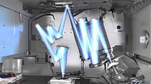
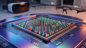
The increasing demand for advanced semiconductor devices with intricate, sophisticated designs has heightened the complexity of integrated circuits (ICs). As IC designs become increasingly complex, traditional lithography methods encounter limitations in resolution and pattern fidelity. Extreme ultraviolet (EUV) lithography addresses these challenges by enabling the fabrication of smaller, more intricate patterns with shorter wavelengths. This technology provides superior resolution and precise control over critical dimensions, meeting the requirements for advanced IC designs. Extreme ultraviolet (EUV) lithography enables the production of next-generation, high-performance chips with highly complex patterns and dense multilayer structures that are critical for advanced semiconductor devices.
"The foundries segment is projected to record the highest CAGR from 2026 to 2032."
The foundries segment is projected to grow at the highest CAGR during the forecast period, driven by strong demand for advanced logic nodes from applications such as artificial intelligence, high-performance computing, and data centres. Increasing fabless semiconductor design activity and outsourcing of advanced-node production are accelerating capacity expansion at leading foundries, supporting higher EUV tool deployment. Continued investments in cutting-edge process technologies and high-volume manufacturing further reinforce the rapid growth of the foundries segment in the extreme ultraviolet (EUV) lithography market.
"Foundries dominated the extreme ultraviolet (EUV) lithography market in the Asia Pacific region in 2025."
Foundries dominate the market in the Asia Pacific region due to the region's intense concentration of leading-edge semiconductor manufacturing hubs, particularly in Taiwan and South Korea. Major foundries are the primary adopters of EUV technology to support advanced process nodes, driving the majority of EUV tool utilisation, component demand, and related investments. Their large-scale production volumes, continuous node migration, and long-term capital expenditure commitments position foundries as the central drivers of EUV lithography deployment and market growth across the Asia Pacific.
"South Korea is projected to exhibit the highest CAGR during the forecast period."
South Korea is projected to register the highest CAGR in the global extreme ultraviolet (EUV) lithography industry during the forecast period, driven by substantial investments in advanced semiconductor manufacturing and aggressive technology roadmaps. The continued expansion of leading-edge logic and memory production, rising adoption of EUV at advanced nodes, and sustained capital expenditure to enhance process efficiency and yield are all accelerating market growth. The country's focus on strengthening semiconductor competitiveness and supporting next-generation manufacturing technologies further reinforces its high-growth outlook in the extreme ultraviolet (EUV) lithography market.
Key Players
The report profiles the key system provider-ASML (Netherlands), as well as key component providers in extreme ultraviolet (EUV) lithography companies such as KLA Corporation (US), ZEISS Group (Germany), TRUMPF (Germany), AGC Inc. (Japan), Lasertec Corporation (Japan), HOYA Corporation (Japan), Applied Materials, Inc. (US), Ushio Inc. (Japan), NTT Advanced Technology Corporation (Japan), ADVANTEST CORPORATION (Japan), SUSS MicroTec SE (Germany), Rigaku Holdings Corporation (Japan), Tekscend Photomask (Japan), and ADVANTEST CORPORATION (Japan).