Thermo Fisher’s Helios MX1 Brings True 3D Insight Into the Fab as Semiconductor Complexity Surges
28 November 2025 |
Interview
Mark Najarian explains how fab-ready plasma FIB-SEM, automation, and data-driven workflows are redefining structural metrology for next-generation logic, memory, and advanced packaging.

As the semiconductor world marches into an era of extreme integration, vertically stacked designs, and unforgiving process windows, structural visibility has become nothing short of a competitive advantage. Traditional lab-bound 3D metrology, with its wafer-breaking rituals and slow feedback cycles, can no longer keep pace with the demands of high-volume manufacturing. Speaking to Semicon Leaders Asia, Mark Najarian, Product Marketing Manager Fab Solutions at Thermo Fisher Scientific. reflects on the industry’s shifting landscape and the growing urgency for in-fab, high-resolution insight. In this interview, he describes how the Helios MX1 plasma FIB-SEM bridges the gulf between R&D precision and fab-floor speed, empowering engineers to see deeper, respond faster, and maintain control as device architectures stretch into new dimensions
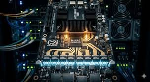
"As semiconductor architectures grow more intricate and vertically stacked, achieving rapid insight into buried structures and subsurface defects has become critical to yield and time-to-market. Traditionally, high-resolution 3D metrology and failure analysis were confined to R&D labs, requiring wafer breakage and time-intensive workflows. Thermo Fisher Scientific responded to this challenge with the Helios MX1 PFIB-SEM, a system designed to bring lab-quality 3D analysis into the fab. By combining plasma FIB milling, high-resolution SEM imaging, and full automation, the Helios MX1 enables fab engineers to inspect, measure, and act faster than ever. Supporting logic, memory (3D NAND, DRAM, 3D DRAM), and advanced packaging including HBM, it is increasingly used as a ground-truth tool for inline process control and defect analysis. As 3D scaling inflections deepen, the role of the Helios MX1 continues to expand across critical semiconductor sectors.
The semiconductor industry today is grappling with the unprecedented complexity of materials, architectures, and integration schemes. Traditional metrology approaches are being pushed to their limits, particularly as 3D integration and atomic-level precision become the new normal. Helios MX1 was conceived to bridge the widening gap between lab-based capabilities and the demands of high-volume manufacturing. It is more than just a tool—it is an enabler of data-driven decision-making and accelerated process optimization, helping fabs remain agile in the face of intense technological inflection."
What inspired Thermo Fisher to bring high-resolution 3D metrology, traditionally used in laboratories, directly into the fabrication environment? How does the Helios MX1 overcome the practical and environmental challenges of such integration?
Shrinking geometries and increasingly three-dimensional device structures have significantly raised the bar for metrology and defect analysis. Historically, engineers relied on lab-based tools for such high-resolution insights, sending wafers to central facilities where they might be subjected to manual cross-sectioning, slow turnaround, and fragmented feedback loops. This model became a bottleneck as fabs demanded faster learning cycles, quicker yield ramps, and more agile responses to process excursions.
Thermo Fisher recognized that enabling in-fab access to 3D structural data could dramatically change the pace and efficacy of process control. The inspiration behind Helios MX1 was to democratize advanced metrology, putting powerful, previously lab-bound capabilities directly into the hands of fab engineers. This approach facilitates same-day feedback and closes the loop between observation, analysis, and action.
Engineering the Helios MX1 to be fab-compatible required thoughtful innovation across hardware and software. The system includes a sealed FOUP-compatible front end for 300 mm wafer handling, cleanroom-compatible vacuum systems, and robust shielding against vibration and electromagnetic interference. Its plasma FIB source enables fast, clean milling without the risk of gallium contamination. Internally, in-situ calibration and smart monitoring of KPIs ensure consistent metrology performance even under demanding production conditions. Importantly, the system integrates seamlessly with fab automation environments via standard SECS/GEM protocols, so it behaves like any other inline tool.
With Helios MX1, fab engineers no longer need to compromise between speed and insight—they gain direct access to volumetric data that informs critical decisions during ramp and high-volume production. This also reduces reliance on external labs, streamlining workflows and making critical structural insights available in real time, where and when they’re needed most.
Could you elaborate on how automated 3D reconstruction in the Helios MX1 accelerates “time-to-data”? What measurable improvements in speed, precision, or analytical throughput have early adopters reported so far?
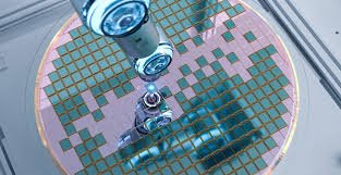
Time-to-data is a key metric in today’s advanced fabs. The sooner an engineer can visualize buried structures or defects, the faster they can respond, tune processes, and avoid scrap. The Helios MX1 addresses this need head-on by combining high-throughput argon plasma FIB milling with a fully automated 3D reconstruction pipeline.
Argon PFIB delivers up to 20 times the throughput of conventional gallium FIB systems, enabling large volumes of material to be removed rapidly with minimal artifacts. This efficiency alone greatly reduces the time spent on physical preparation. Once the volume is acquired, the system’s software performs slice alignment, volume stitching, and reconstruction without the need for expert intervention. This end-to-end automation allows engineers to move from sample loading to data visualization within a matter of hours, dramatically shrinking the cycle from problem detection to root-cause understanding.
One of the most transformative capabilities is virtual slice extraction. A single 3D dataset can serve as a proxy for multiple conventional cross-sections—orthogonal cuts, delayering sequences, diagonal mills—that would otherwise be performed manually and sequentially. Engineers can navigate through the reconstructed volume in any orientation, select planes of interest, and extract metrology-relevant information with unprecedented flexibility.
In practice, this means a single Helios MX1 run can replace up to five traditional sample prep and analysis steps. During process development, this allows teams to quickly isolate failure mechanisms, validate structural targets, or explore the impact of upstream variations—all without the overhead of multiple lab submissions. Furthermore, the ability to virtually re-slice and re-analyze stored volumes enables deeper insight over time, supporting longer-term process development and yield improvement initiatives.
While measurement precision in 3D reconstruction depends on imaging conditions, material contrast, and voxel resolution, the system delivers robust and repeatable datasets suitable for structural correlation and virtual metrology. For KPI tracking and system validation, a standard sample has been adopted to track metrology precision. These performance metrics build user trust and support adoption in highly regulated manufacturing environments.
By unifying high-throughput milling, automated reconstruction, and intuitive analysis, Helios MX1 redefines the speed and accessibility of 3D insight in the fab.
What makes the Helios MX1 truly “fab-ready” compared to other FIB-SEM systems? Were there specific design or engineering considerations taken to ensure performance stability and contamination control within production cleanrooms?
Being “fab-ready” involves more than simply placing a lab tool in a cleanroom. The Helios MX1 was meticulously engineered to meet the automation, reliability, and integration demands of high-volume semiconductor manufacturing.
One core element is the 300 mm wafer handling system, which includes FOUP-compatible loading, wafer pre-alignment, and recipe-based site navigation. This allows the tool to operate fully automated—dispatching wafers, executing analysis, and returning data to the MES without human intervention. The system is designed for sustained uptime and minimal operator dependency, supporting round-the-clock metrology operations.
In terms of wafer contamination, one major design consideration was eliminating gallium from the process. The Helios MX1 uses argon and xenon plasma sources instead of gallium, enabling high-speed milling while avoiding the implantation of foreign species that could interfere with device behavior. Our customers have found methods to return wafers to the process flow after analysis, depending on their internal specifications and contamination control strategies.
Moreover, customers are addressing contamination control by carefully selecting which process steps to inspect and when to perform inline metrology. This targeted approach helps balance analytical value with process safety. By tailoring inspection strategies to their process flow, fabs ensure that analysis remains both informative and non-disruptive.
From a metrology perspective, Helios MX1 features automated in-situ alignments and calibrations, along with smart KPI tracking for parameters like beam coincidence, image sharpness, focus, and stigmation. These systems allow the tool to self-monitor and self-correct, maintaining consistent performance with minimal user input. The metrology precision and reproducibility are validated using built-in standards and process control wafers.
Additionally, fabs have found that Helios MX1 enables in-line re-entry of wafers and targeted sampling at specific process steps. This facilitates iterative analysis across a wafer’s journey, enhancing visibility into process interactions without needing destructive sample prep at each stage. The ability to non-destructively revisit and re-analyze wafers empowers smarter process tuning and helps reduce cycle times during development.
As semiconductors increasingly power domains such as AI computing, automotive electronics, and healthcare, how does the Helios MX1 help manufacturers achieve tighter process control and defect visibility in these complex and sensitive device architectures?
Today’s semiconductors are built for a wide array of mission-critical applications—from high-performance computing and AI to autonomous driving and medical devices. These domains demand not just higher performance but also greater reliability, uniformity, and failure resilience.
The Helios MX1 plays a central role in enabling this vision by providing a deep look into the structures that underpin performance and yield. For logic devices featuring advanced transistor architectures like gate-all-around and finFETs, the Helios MX1 enables direct observation of fin profiles, gate spacers, and contact integrity. In AI chips with aggressive scaling and complex interconnect stacks, understanding the physical alignment and structural fidelity of these features is critical.
In memory applications like 3D NAND and emerging 3D DRAM, the Helios MX1 allows engineers to analyze vertical channels, assess etch quality across dozens of stacked layers, and detect subtle profile drifts or voids that may impact bit yield. The ability to observe these structures volumetrically—and correlate that insight with electrical behavior—provides a new dimension of process control. This capability is especially valuable in high-aspect-ratio structures where traditional techniques fall short.
For advanced packaging, including high bandwidth memory and chiplets, the Helios MX1 supports metrology & defect analysis in TSVs, micro-bumps, and die interfaces. Engineers can evaluate bonding quality, inspect for delamination, and measure structural dimensions across package layers. This is particularly valuable in markets like automotive and healthcare where mechanical integrity and long-term reliability are paramount.
By enabling high-resolution, in-fab structural analysis, Helios MX1 empowers fabs to catch defects earlier, tune processes with greater precision, and accelerate the delivery of robust, next-generation devices. It is a tool not only for analysis but for active process refinement across the semiconductor lifecycle.
With automation and AI-driven analysis becoming central to productivity gains, how do you see the Helios MX1 transforming the role of process engineers and metrology experts within fabrication plants?
Helios MX1 marks a shift in how engineers interact with advanced analysis tools. It moves them away from dependence on external labs and manual workflows toward autonomous, real-time insight within the fab.
Through automated sample navigation, beam alignment, image acquisition, and reconstruction, the tool minimizes human variability and reduces analysis cycle time. Engineers can focus less on setup and execution, and more on data interpretation and decision-making. This improves efficiency, especially in fabs that are operating with lean technical staffing.
The system’s intuitive software interface, coupled with web-based review dashboards, allows cross-functional teams to interact with 3D datasets, annotate features of interest, and extract measurements collaboratively. Knowledge sharing and alignment between process, integration, and failure analysis teams becomes easier.
As machine learning continues to evolve, Helios MX1 will benefit from AI-assisted workflows that guide users toward regions of interest, suggest slice orientations, or prioritize anomaly review. While human judgment remains essential, these enhancements enable engineers to cover more ground with higher confidence. By incorporating smart suggestions and automated error detection, the tool helps reduce interpretation fatigue and accelerate time-to-resolution.
Overall, Helios MX1 empowers process and metrology experts to act with greater speed, autonomy, and strategic impact, helping fabs accelerate learning cycles and maintain control over increasingly complex process windows. This evolution in role and capability marks an important step toward the future of smart, adaptive manufacturing.
Looking ahead, what are Thermo Fisher’s next strategic steps in advancing semiconductor characterization—particularly regarding hybrid metrology, in-line analytics, or AI-enabled inspection platforms?
Thermo Fisher’s roadmap builds on the foundation established by the Helios MX1, with a strong emphasis on integration, automation, and insight generation across metrology and inspection ecosystems.
- Hybrid Metrology: The company is exploring integrated and complimentary workflows that leverage Helios MX1’s 3D data to improve the development of optical and X-ray model optimization. By aligning volumetric ground-truth measurements with higher-throughput, in-line techniques, fabs can benefit from calibrated, accurate process monitoring at scale. This approach bridges resolution and speed, offering the best of both worlds. As the industry embraces more complex stacks and materials, hybrid metrology will be essential to correlate data across toolsets and validate critical steps with confidence.
- Inline Analytics: As data volumes grow, Thermo Fisher is investing in smart analytics engines that provide real-time trend detection, SPC monitoring, and correlation across datasets. This enables process engineers to receive alerts and insights faster, and integrate metrology findings directly into process control loops. Future systems may leverage predictive modeling to preemptively identify process drifts or shifts, reducing the frequency and impact of yield excursions.
- AI-Enabled Inspection: While Helios MX1 focuses on defect analysis—revealing structure, location, and root cause of buried or volumetric issues future platforms may incorporate AI to further streamline workflows. This could include guided navigation, intelligent slice selection, and automated identification of recurring structural patterns. Rather than simply classifying defects, the emphasis is on understanding their formation and impact in context. These tools will allow fab teams to close the gap between detection and correction, leveraging AI as a partner in proactive process refinement.
Thermo Fisher is also exploring new modalities and complementary techniques that extend beyond imaging, such as correlative spectroscopy and electrical probing, further enhancing the value of structural insight. These developments will ensure that the company remains a key enabler of next-generation manufacturing and device innovation.