Baya Systems Targets Japan’s AI and Chiplet Market with Advanced Data-Movement Technology
08 September 2026 |
Interaction
Japan expansion strengthens Baya’s presence in AI, HPC, automotive and heterogeneous computing as demand grows for scalable fabric IP and chiplet architectures.
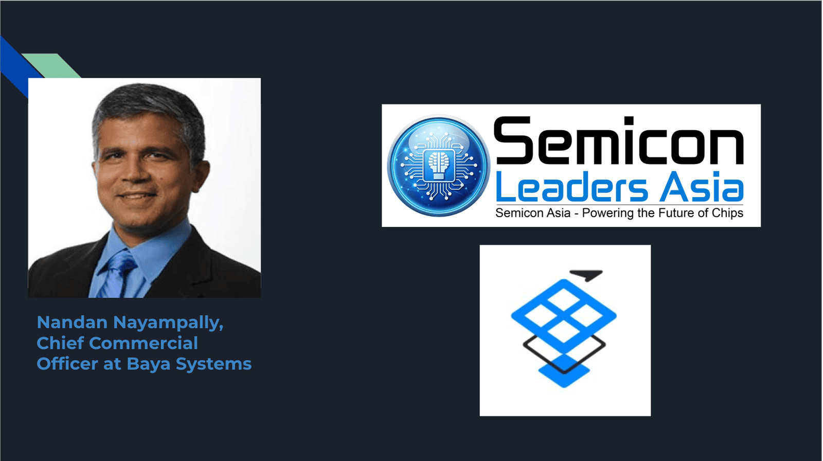
In this exclusive interview, Semicon Leaders Asia speaks with Nandan Nayampally, Chief Commercial Officer at Baya Systems, about the company’s expansion into Japan and the growing opportunities across the country’s semiconductor ecosystem. Nayampally shares his insights into the rising demand for AI, HPC, automotive and chiplet-based architectures, the importance of efficient data movement in increasingly complex semiconductor systems, Baya Systems’ collaboration with Tenstorrent, and the company’s broader strategy for strengthening partnerships across Japan and the wider APAC market.
1: Baya Systems is expanding into Japan as demand for AI, HPC, and chiplet-based architectures grows. What specific opportunities in the Japanese semiconductor ecosystem are driving this expansion?
Japan is interesting because several important shifts are occurring simultaneously. Japan has been at the forefront of HPC and supercomputing, and I enjoyed the engagement when they built the Arm-based Fugaku supercomputer. Japan is now investing aggressively in advanced semiconductor capability, AI infrastructure, and the broader ecosystem needed to design and deploy increasingly sophisticated compute systems. Japan’s Ministry of Economy, Trade and Industry has set out a framework providing more than ¥10 trillion in public support for AI and semiconductors through fiscal 2030 to catalyse more than ¥50 trillion in public-private investment over a decade. Japan is also actively supporting AI compute resources and advanced semiconductor R&D.
Baya has very relevant and critical technology that supports these initiatives, and we’ve already taken the opportunity to translate this into a concrete technology collaboration. As part of our work with Tenstorrent, a next-generation test chip under development in Japan will incorporate Baya’s WeaveIP™ fabric. That work aligns closely with Japan’s broader push toward advanced semiconductor technologies and next-generation AI acceleration. The synergies are evident with Baya providing the data-movement architecture needed to connect increasingly sophisticated compute, memory and I/O subsystems.
For Baya, the opportunity sits at the intersection of those investments and a fundamental architectural change in semiconductors. AI and HPC systems are no longer simply about adding more compute. The challenge is moving the right data between CPUs, accelerators, memory, I/O, and, increasingly, multiple chiplets at the right bandwidth and latency, and within practical power and area limits. That is the system-level problem we were created to address. Our Japan expansion brings active local technical and field resources closer to semiconductor companies,
foundries, and technology leaders working on AI, HPC, automotive, and advanced chiplet-based designs.
Chiplets are particularly important. Japan’s semiconductor agenda increasingly includes heterogeneous integration and chiplet technologies, while the global UCIe ecosystem is establishing an open framework for die-to-die interoperability. That creates an environment in which more companies can assemble differentiated systems from specialised compute, memory and I/O elements, but it also increases the complexity of system architecture and data movement.
We also see strong alignment with Japan’s automotive and industrial strengths. METI’s Mobility DX work is advancing software-defined vehicles, AI-enabled autonomous driving, and more digitised development processes. These platforms are becoming heterogeneous compute systems in their own right, and their requirements for predictable performance, efficiency, reliability, and scalability are increasingly difficult to meet with isolated point products.
Finally, Japan values deep engineering collaboration. And so does Baya. What has made Baya successful is that we engage early with visionary leaders in the industry, understand what they care most about, work with architecture teams, understand workloads and constraints, and help these lead customers explore the system before they commit to silicon. The opportunity is therefore both commercial and technical: to become part of the local design ecosystem as Japan develops its next generation of AI, HPC, automotive and chiplet systems.
2: Baya’s WeaveIP™ fabric IP is designed to enable scalable, software-defined data movement across advanced SoCs and chiplet architectures. What differentiates WeaveIP from conventional semiconductor fabric and interconnect solutions?
The biggest difference is that we view fabric as a core of the system architecture in single and multi-die systems, which needs to be designed and optimised with a full view of the end-system outcome, with the target workloads and KPIs that are met right from the start. In advanced SoC or multi-chiplet designs, the design and partitioning of the fabric may need advanced analysis and extreme flexibility. It determines how efficiently compute, memory, and I/O can work together, so it has to be explored and optimised alongside the rest of the system. More importantly, it needs to be designed to be rapidly and efficiently realised in silicon, and with the chip-to-chip and die-to-die complexity resolved. Baya focuses on solving all these challenges.
That is why WeaveIP and WeaverPro are co-designed for a seamless workflow. WeaverPro lets an architecture team model workloads, explore cache and fabric structures, analyse bottlenecks, and evaluate KPIs such as bandwidth, latency, and congestion before committing to implementation. FabricStudio adds static analysis, dynamic simulation, and physical-design constraints, enabling the team to move from architecture exploration to an implementation that is correct by construction and designed to be deadlock-free.
The second difference is architectural flexibility. WeaveIP is a portfolio built around a common scalable transport approach rather than a single protocol-specific network. The portfolio includes coherent fabric, non-coherent fabric, protocol-neutral AI fabric, and non-blocking switch fabric. This allows customers to build around the actual communication needs of their system rather than forcing all traffic into the same architectural assumption. It also provides a common foundation that can be adapted and reused across different SoCs, chiplets, and product generations as system requirements evolve.
Third, our technology is built to integrate chiplets from the outset. Once a design spans multiple dies, architects must consider topology, physical boundaries, bandwidth allocation, protocol behaviour, die-to-die latency, and how the system will scale across multiple product generations. UCIe is helping the industry standardise key elements of the die-to-die interface, but architects still need to design the data-movement system above and around it. A standardised die-to-die link solves the physical connectivity problem; it does not by itself determine how data should move efficiently across the overall system. That is where software-defined fabric architecture becomes valuable.
The Tenstorrent work gives us a concrete proof point. We reported that our collaboration with Tenstorrent achieved up to 66% higher throughput, 75% lower latency than their previous customised solution’s peak bandwidth, and a 50% reduction in silicon area for that specific design. The important lesson is not that every customer will see identical numbers. Treating the fabric as a system-level optimisation problem can create meaningful improvements in performance, latency, and silicon efficiency simultaneously.
So, in simple terms, conventional interconnect asks, “How do I connect these blocks?” We start one level higher: “What data has to move, under what workloads and constraints, and what fabric architecture will let the entire system perform the way the customer intends?” Then we carry those architectural decisions through toward physical implementation.
3: Baya is collaborating with Tenstorrent on a test chip incorporating WeaveIP. What does this collaboration demonstrate about the role of software-defined fabric IP in building next-generation AI and high-performance computing architectures?
The Tenstorrent collaboration is important because it connects architecture exploration to real silicon development. Tenstorrent first licensed Baya’s WeaveIP technology in 2024 for its AI and RISC-V chiplet solutions. At the time, Tenstorrent highlighted the ability to work from top-level architecture through performance modelling, transport, quality of service, and cache coherency rather than treating the interconnect as an isolated block. We’ve taken that collaboration another step forward and are now working on a test chip that incorporates WeaveIP. That illustrates how software-defined fabric can become part of the design methodology, not simply another IP selection decision.
AI and HPC architectures are extraordinarily dynamic. Workloads change, accelerator counts grow, memory configurations evolve, and chiplet partitioning can change from one product
generation to the next. A fabric optimised only for a single static configuration can quickly become a constraint. A software-defined approach lets architects explore different topologies, bandwidth allocations, traffic behaviours, and implementation choices before RTL is frozen, and then deploy a fabric architecture that reflects those decisions. Baya’s WeaverPro flow was designed specifically to connect that architectural exploration with WeaveIP deployment. The important point is that the fabric can be shaped around the workload and helps build the optimal system architecture.
The collaboration also shows why this matters for chiplets. Tenstorrent’s broader platform includes TT-Ascalon RISC-V CPU IP and Tensix AI accelerator technology. As systems combine more heterogeneous elements, the efficiency of the communication layer increasingly determines how much useful performance the system can extract from the compute designed into it. Adding more compute does not automatically translate into more system performance if data cannot move efficiently among those elements. The fabric therefore becomes an increasingly important part of scaling the architecture.
Japan makes that proof point particularly relevant. Tenstorrent already has an established Japanese engineering and AI-compute presence, including operations in Tokyo and Osaka, as well as work with Japan’s semiconductor ecosystem. Our collaboration therefore sits naturally within a market that is actively exploring advanced AI, RISC-V, and chiplet architectures.
We should also be precise about where the project stands. The test chip is currently under development. We will share additional milestones when the companies are ready. What we can say now is that the project represents an important step toward demonstrating how software-defined data movement can be designed as part of the compute architecture itself.
4: As semiconductor designs become increasingly complex and chiplet architectures gain momentum, how does Baya help customers reduce design complexity while improving scalability, performance, and system efficiency?
The paradox of modern semiconductor design is that modularity can make a system easier to compose conceptually while making the architecture much harder to optimise. Chiplets give designers more freedom to combine compute, accelerators, memory, and I/O. Still, every new boundary introduces questions about bandwidth, latency, coherency, topology, physical implementation, and how traffic will behave under real workloads.
Our approach is to answer those questions earlier and in a more integrated way. Rather than treating architecture, fabric design, and physical implementation as separate steps, Baya connects them in a common workflow.
With WeaverPro, architects can define the system and investigate cache and fabric choices before the design is locked down. CacheStudio focuses on cache and memory hierarchy behaviour, including workload-driven analysis of parameters such as miss rates, snoop behaviour, and bandwidth requirements. FabricStudio then uses system requirements, topology choices,
and physical constraints to explore the fabric microarchitecture, identify bottlenecks, and generate implementation collateral. We describe FabricStudio as combining static analysis and dynamic simulation to enable teams to validate KPIs, optimise topology, and ensure deadlock-free operation before implementation.
That changes the development loop. Instead of discovering late in the flow that the fabric cannot sustain a traffic pattern or that the intended topology creates an implementation problem, teams can ask those questions while architectural changes are still relatively inexpensive. That can reduce iteration, shorten the path from architecture to implementation, and make performance and efficiency tradeoffs visible much earlier.
The second part is reuse and scalability. WeaveIP uses a common scalable transport approach across several types of fabric. Calico addresses flexible non-coherent connectivity; Cashmere extends to scalable coherent systems; Chiffon-AI addresses protocol-neutral AI data movement; and NeuraScale addresses non-blocking switching for AI scale-up and scale-out. The intent is to let teams retain a familiar architecture and tool methodology while adapting the fabric to different products and communication requirements. That becomes increasingly valuable as customers move from one SoC or chiplet configuration to another and need to scale the architecture without starting over each time.
Physical awareness is equally important. A theoretically elegant network is not very useful if it is difficult to place, route, or scale across chiplets. FabricStudio therefore incorporates floorplan and physical design constraints into the architectural process and produces implementation-oriented outputs. That helps bridge a gap that traditionally exists between system architects and implementation teams. It also helps ensure that the architecture being optimised in software is grounded in what can realistically be implemented in silicon.
Ultimately, reducing complexity does not mean hiding the engineering decisions. It means making those decisions visible earlier, choices made better with the right data and automation to reduce manual error and to improve scale. Customers still control the architecture. Our role is to give them a faster way to explore it, prove it, design it, and deploy it, so that scalability, performance, and efficiency are built into the system rather than debugged later.
5: Japan is investing heavily in advanced semiconductor manufacturing and AI infrastructure. Which application areas — AI accelerators, HPC, automotive, or other advanced SoCs — do you see generating the strongest demand for Baya’s technology?
We expect AI acceleration and AI/HPC infrastructure to create the most immediate demand, with automotive and other sophisticated heterogeneous SoCs representing a very important second wave. That prioritisation reflects where system-level data movement is becoming most difficult and where Japan is directing substantial technology investment.
AI systems are the clearest example. Adding compute only helps when memory and interconnect can feed it efficiently. Training and inference systems are scaling across larger numbers of accelerators, which is why the industry is developing open scale-up technologies such as UALink and why the requirements for bandwidth, latency, and network efficiency are increasing so rapidly. UALink’s public specification is explicitly designed around low-latency, high-bandwidth communication among accelerators and switches in AI computing pods. We address that broader data-movement challenge with its AI-oriented fabric portfolio, including Chiffon-AI and NeuraScale.
Japan is also investing directly in the compute side of AI. METI and NEDO’s GENIAC program supports access to the compute resources needed to develop foundation models. At the same time, Japan’s broader AI-semiconductor framework is designed to stimulate large-scale investment across both hardware and AI. That makes AI accelerators, AI servers, switching, and HPC-class silicon a natural priority.
We also see edge AI as particularly relevant in Japan. Advanced semiconductor programs are targeting edge inference, including generative AI, for applications such as industrial robotics and automotive systems. Those workloads bring AI processing closer to where data is generated and often combine CPUs, accelerators, memory, and specialised I/O under tight power, latency, and area constraints. This is exactly the kind of heterogeneous architecture where efficient data movement becomes critical.
Automotive is different but equally interesting over the longer term. Japan’s Mobility DX Strategy emphasises software-defined vehicles, AI-driven autonomous driving development, and more digitised development processes. Automotive SoCs are increasingly heterogeneous systems with CPUs, accelerators, safety islands, I/O, memory, and complex real-time traffic. They need scalability, but they also demand predictability, robustness, and long lifecycle support. Those requirements align well with the architectural approach behind our coherent and non-coherent fabrics.
Beyond those categories, we see opportunity anywhere the SoC is becoming a system rather than a collection of blocks: networking, data-centre infrastructure, and other high-performance custom silicon.
The common denominator is not a particular vertical. It is architectural complexity. When data movement becomes a first-order constraint on performance, power, area, or scalability, software-defined fabric becomes increasingly valuable.
6: Following its expansion across North America, Europe, and India, how does Japan fit into Baya’s broader APAC growth strategy, and what are the company’s priorities for building partnerships with Japanese semiconductor companies and technology leaders?
Japan is an important strategic node in our global model because it brings together advanced semiconductor design and manufacturing capabilities, automotive leadership, AI investment, and a deep engineering culture. Within APAC, it complements our strong engineering presence
in India by bringing us closer to customers, partners, and advanced semiconductor programs in one of the region’s most important technology markets.
Baya has been expanding around major centres of semiconductor innovation. We are headquartered in Santa Clara, operate in Austin and Bengaluru, and have opened our European office in Cambridge. Our next phase in Japan is to build our footprint through customer engagements, ecosystem partnerships, and industry events, supported by active local technical and field resources. That is the model we expect to follow in APAC: combine local market and customer engagement with access to Baya’s broader global engineering organisation.
Our priority is customers. Fabric architecture is most valuable when the conversation begins early, so we want Japanese design teams to have direct access to people who can discuss workloads, cache hierarchy, fabric topology, chiplet partitioning, and implementation. The goal is to engage upstream in the architecture process rather than only at the point of IP selection.
The second priority is ecosystem collaboration. No company builds an advanced SoC alone. CPUs, accelerators, memory, die-to-die interfaces, packaging, physical IP, design services and software all have to work together. Our collaboration with Tenstorrent is one example of that model. Tenstorrent has an established presence in Japan and has publicly described collaborations across the country’s AI and semiconductor ecosystem. We see similar opportunities to work alongside semiconductor companies, foundries, IP providers, design partners, and other technology leaders as the local ecosystem evolves.
Third, we want to participate in the technical ecosystem around open and modular architectures. Standards such as UCIe are making chiplet interoperability more practical, while AI-scale connectivity initiatives such as UALink are expanding the architectural options available to system developers. Our role is to help designers leverage that modularity without letting system-level data movement become the next bottleneck.
And finally, this has to be a long-term commitment. Japan’s semiconductor revival is not a single product cycle. METI’s semiconductor and AI framework extends through 2030, and the country is investing simultaneously in manufacturing, AI infrastructure, engineering talent, and next-generation applications. We want to build relationships on the same horizon. For us, success in Japan means becoming a trusted part of the local design ecosystem, not simply establishing a sales presence.