Wafer-Scale P-Type 2D Semiconductor Clears Key Hurdle for Next-Generation Chips
New research advances scalable p-type 2D materials, supporting future CMOS technologies and more advanced semiconductor architectures.
Researchers have made progress towards addressing one of the major challenges facing two-dimensional semiconductor technology: developing a stable, high-performance p-type material that can be produced across wafer-scale substrates. The advance could support the development of future complementary metal-oxide-semiconductor (CMOS) technologies as the semiconductor industry explores alternatives to conventional silicon scaling.
Two-dimensional semiconductors have attracted significant interest because their extremely thin structures can provide strong electrostatic control and potentially enable transistors to be scaled beyond the limitations of conventional materials. However, while a range of n-type 2D semiconductor materials have been demonstrated, suitable p-type alternatives remain considerably more difficult to develop. This imbalance has limited the ability to build practical complementary circuits using 2D materials.
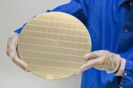
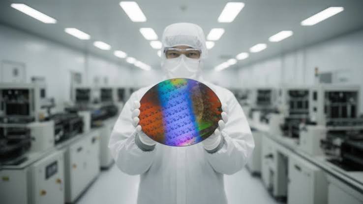
The latest work focuses on achieving p-type semiconductor films over an entire wafer rather than producing isolated devices or small material samples. This distinction is important for eventual semiconductor manufacturing, where material uniformity, reproducibility and scalability are essential requirements for integrating large numbers of transistors into functional circuits.
Recent research has demonstrated wafer-scale p-type 2D semiconductor platforms with controlled material properties and transistor performance. One reported approach uses four-inch 2H-MoTe₂ films, enabling the fabrication of medium-scale integrated circuits. The researchers achieved reproducible p-type transistor characteristics, including on/off ratios of around 10⁵ and carrier mobility of approximately 7 cm²/V·s under low operating voltages. They also demonstrated a 140-transistor full-adder circuit, highlighting the potential for moving beyond individual experimental devices towards more complex 2D integrated electronics.
Another recent development has focused on wafer-scale monolayer WSi₂N₄, a p-type 2D semiconductor being investigated for its electrical, mechanical and thermal characteristics. Researchers reported large-area films produced through chemical vapour deposition, together with control over carrier doping. The resulting material demonstrated a bandgap of approximately 2.25 eV, an on/off current ratio of 5.4 × 10⁴ at lower doping levels and an on-state current density of around 150 μA/μm under heavier doping. The material also showed high mechanical strength and stability, characteristics that could be relevant to future integrated-device applications.
The development of wafer-scale p-type materials is particularly significant because complementary logic requires both n-type and p-type semiconductor channels. Conventional CMOS relies on this complementary structure to achieve efficient digital logic, meaning that the lack of reliable p-type 2D materials has remained a major obstacle to the wider adoption of 2D semiconductor platforms.
Beyond transistor performance, manufacturing compatibility is another important consideration. For 2D materials to become commercially relevant, researchers will need to demonstrate consistent deposition or growth, controlled thickness, low defect densities, reliable contacts and integration with existing semiconductor manufacturing processes. Research in the field is therefore increasingly shifting from material discovery towards wafer-scale synthesis, device integration and circuit-level demonstrations.
The progress could eventually contribute to new approaches for advanced CMOS, heterogeneous integration and monolithic three-dimensional semiconductor architectures. Because 2D materials can be formed with atomically thin channels, they are being investigated for applications where conventional transistor scaling is becoming increasingly challenging. Their properties could also make them suitable for integrating additional electronic functionality in tightly constrained areas of a chip.
For the semiconductor industry, the ability to produce uniform p-type 2D semiconductor layers over large substrates represents an important step towards translating laboratory-scale demonstrations into more realistic manufacturing environments. Further work will nevertheless be required to improve material quality, device consistency, contact performance and integration with established fabrication processes.
The broader research effort demonstrates how 2D semiconductor technologies are evolving from proof-of-concept devices towards increasingly sophisticated integrated circuits. Although significant engineering and manufacturing challenges remain, wafer-scale p-type materials could provide an important building block for future complementary electronics and help expand the range of materials available for next-generation chip architectures.