Kioxia and Sandisk Unveil 9th-Generation 2Tb QLC NAND for AI Data Centres
New 3D flash technology delivers 4.8Gb/s interface speeds, higher bandwidth and improved power efficiency to meet growing AI storage demands.
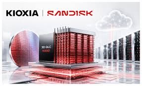
Kioxia Corporation, a subsidiary of Kioxia Holdings Corporation (TOKYO: 285A), and Sandisk Corporation (Nasdaq: SNDK) today unveiled their new 9th-generation, high-performance 2Tb QLC 3D flash memory technology designed to support the growing storage demands of AI-driven infrastructure. The technology demonstrates how architectural innovation can help storage advance at the fast pace required by AI-driven workloads, while supporting more capital-efficient manufacturing.
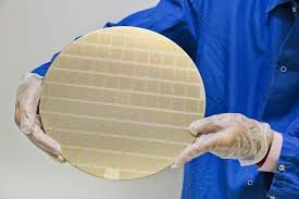
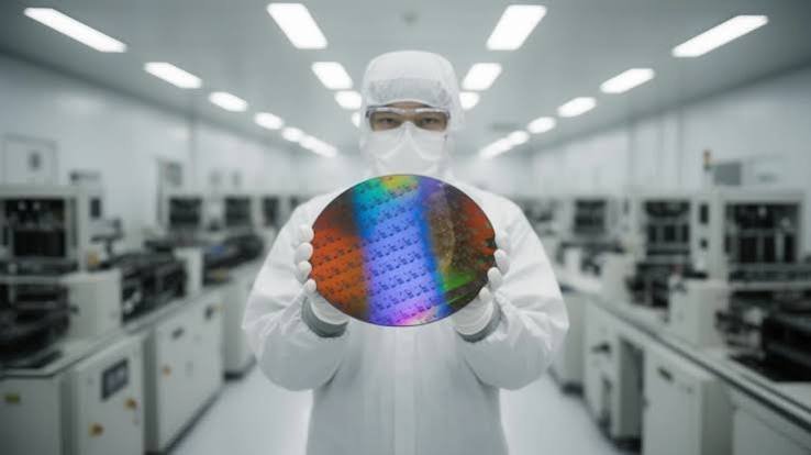
Leveraging the company’s CMOS directly Bonded to Array (CBA) architecture1, the new technology combines an advanced CMOS wafer with a proven memory-array platform, along with significant design and device innovation, to deliver performance improvements and enable faster deployment of advanced storage solutions for cloud and data-intensive applications. Compared with the previous 8th-generation 2Tb QLC, the new technology delivers higher write and read bandwidth due to a 6-plane architecture and performance enhancements and better write and read power efficiency. And it also delivers a NAND interface speed of 4.8Gb/s 2, a 33% improvement over 8th-generation devices.
Chief Technology Officer at Kioxia, Hideshi Miyajima, said, "As AI continues to underpin the advancement of society, its applications are expanding from generative AI to agent-based and physical AI, while the use of data is becoming increasingly diverse and sophisticated. By leveraging its proven memory cell technology together with the latest CMOS technology, Kioxia is accelerating the development of its 9th-generation flash memory. This approach enables us to deliver high performance while keeping investment costs relatively low."
"The rapid adoption of AI is accelerating the transition of storage interfaces, creating demand for memory technologies that can evolve more quickly than in previous technology cycles," said Alper Ilkbahar, Chief Technology Officer at Sandisk. "Our 9th-generation QLC technology demonstrates the unique flexibility of CBA, to accelerate innovation by independently advancing CMOS and memory technologies. We are bringing new capabilities to market more quickly with exceptional capital efficiency."
The introduction of the 9th-generation QLC 3D flash memory technology marks an important milestone in the evolution of the 3D flash memory roadmap and highlights the continued strength of the collaboration between Kioxia and Sandisk. By maximizing the flexibility of their CBA platform, the companies are creating new opportunities for NAND innovation and helping customers address the growing storage demands of the AI era.
- Technology wherein each CMOS wafer and cell array wafer are manufactured separately in their optimized condition and then bonded together.
- 1Gb/s is calculated as 1,000,000,000 bits/second. This value is obtained under our specific test environment and may vary depending on use conditions.
- Product density is identified based on the density of memory chip(s) within the Product, not the amount of memory capacity available for data storage by the end user. Consumer-usable capacity will be less due to overhead data areas, formatting, bad blocks, and other constraints, and may also vary based on the host device and application. For details, please refer to applicable product specifications. The definition of 1KB = 2^10 bytes = 1,024 bytes. The definition of 1Gb = 2^30 bits = 1,073,741,824 bits. The definition of 1GB = 2^30 bytes = 1,073,741,824 bytes. 1Tb = 2^40 bits = 1,099,511,627,776 bits.
- Company names, product names, and service names may be trademarks of third-party companies.