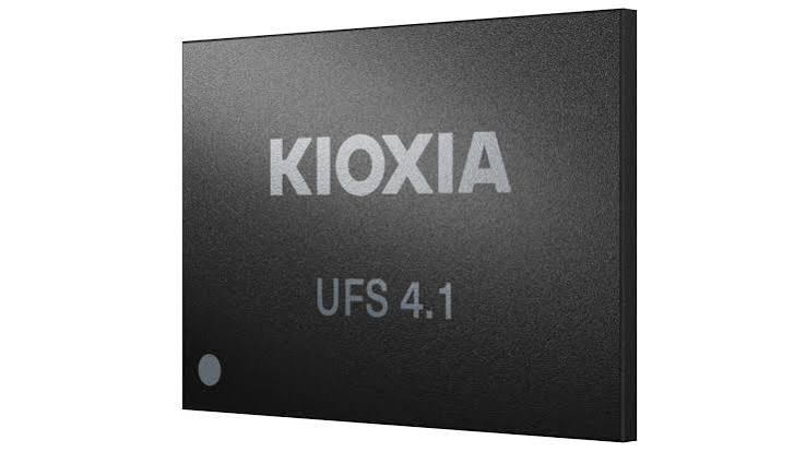
Kioxia Begins Sampling 9th-Generation BiCS FLASH 1Tb TLC Memory for AI Devices
New 230-layer 3D NAND devices deliver 33% faster interface speeds and leverage Kioxia’s dual-axis BiCS FLASH strategy to enhance performance and efficiency for AI-enabled PCs, smartphones, and next-generation storage applications.
Kioxia Corporation, a world leader in memory solutions, announced it has commenced sample shipments of 1Tb (terabit) Triple-Level Cell (TLC) memory devices incorporating its 9th-generation BiCS FLASH™ 3D flash memory technology. The devices are designed to support applications such as AI-enabled PCs and smartphones with low- to mid-level storage capacities that require high performance.
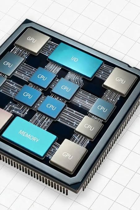
Kioxia continues to pursue a dual-axis strategy based on its innovative CMOS directly Bonded to Array (CBA) technology2 and On-Pitch Select Gate Drain (OPS) technology3. Under its unique dual-axis strategy, Kioxia is simultaneously advancing two distinct product lines: its 9th-generation solutions, which deliver high performance at relatively low investment cost of investing, and its 10th-generation technology, which leverages advanced layer stacking to achieve massive capacity and superior performance.
The new 9th-generation BiCS FLASH™ 1Tb TLC devices, developed using a 230-layer stacking process based on 8th-generation BiCS FLASH™ technology and advanced CMOS technology, deliver a NAND interface speed of 4.8Gb/s, a 33% improvement over 8th-generation devices, matching the performance of 10th-generation devices4.
Guided by its mission of “uplifting the world with ‘memory,’” Kioxia remains committed to driving technological innovation, strengthening global partnerships, and delivering the advanced storage solutions that power modern AI infrastructure.
- These samples are produced for the purpose of checking functionality; actual specifications may differ in mass production.
- Technology whereby each CMOS wafer and cell array wafer is manufactured separately under individually optimised conditions and then bonded together. This technology has been adopted since the 8th-generation BiCS FLASH™ products.
- Technology that makes it possible to shorten the bit line and reduce the word line capacitance by removing unused memory holes. This technology has been adopted since the 8th-generation BiCS FLASH™ products.
- 1Gb/s is calculated as 1,000,000,000 bits per second. This value was obtained in a specific test environment at Kioxia Corporation; the results may vary in actual use depending on the usage conditions.
* Product density is identified based on the density of memory chip(s) within the product, not the amount of memory capacity available for data storage by the end user. Consumer-usable capacity will be lower due to overhead data areas, formatting, bad blocks, and other constraints, and may also vary based on the host device and application. For details, please refer to applicable product specifications. 1Gb = 2^30 bits = 1,073,741,824 bits.
* Read and write speeds are the best values obtained in a specific test environment at Kioxia Corporation; the company warrants neither read nor write speeds in individual devices. Read and write speeds may vary depending on the device used.
* Company names, product names and service names may be trademarks of third-party companies.
* This announcement has been prepared to provide information on our business and does not constitute or form part of an offer or invitation to sell or a solicitation of an offer to buy or subscribe for or otherwise acquire any securities in any jurisdiction or an inducement to engage in investment activity nor shall it form the basis of or be relied on in connection with any contract thereof.
* Information in this document, including product prices and specifications, content of services and contact information, is correct on the date of the announcement but is subject to change without prior notice.