Cognex Launches In-Sight 1750 for AI-Driven Wafer Traceability and Semiconductor Production
New AI-powered wafer identification system helps semiconductor manufacturers improve traceability, reduce production disruptions and maintain throughput across fabrication and packaging operations.
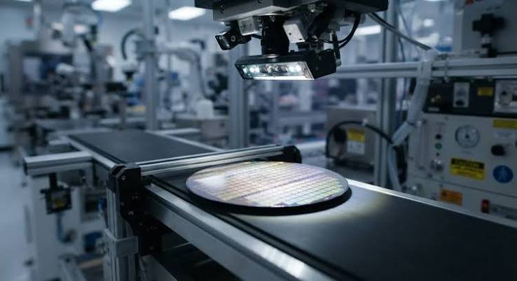
Cognex Corporation (NASDAQ: CGNX), the global technology leader in industrial machine vision, announced the launch of the In-Sight® 1750 Series, a next-generation wafer and panel identification system designed to help semiconductor manufacturers reduce disruptions, improve traceability, and maintain throughput.
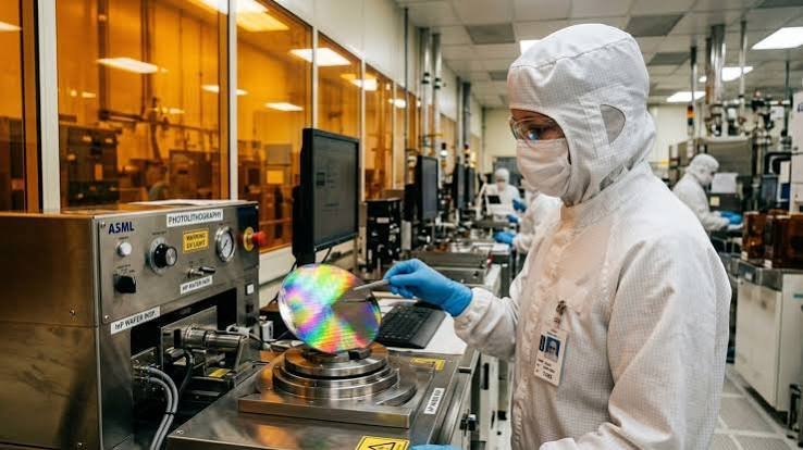
As semiconductor manufacturers expand capacity to support AI infrastructure, advanced computing, and next-generation electronics, the ability to accurately track wafers throughout production has become increasingly important. Even a small number of missed reads can create delays, increase work, and impact equipment efficiency.
The In-Sight 1750 helps manufacturers overcome these challenges by reliably reading many difficult wafer and panel markings and IDs, including various degraded marks and challenging substrates that often require intervention. Building on Cognex's long-standing leadership in wafer identification, the system brings together Cognex's latest AI innovations, advanced imaging, and purpose-built illumination to help manufacturers maintain traceability and throughput in challenging semiconductor environments. The result is often fewer interruptions, more consistent process control, and greater confidence in manufacturing operations.
"Investment in AI infrastructure is driving a new wave of expansion across the semiconductor industry, and chipmakers are being asked to bring new capacity online faster than ever while maintaining the highest quality standards," said Matt Moschner, President and CEO of Cognex. "The In-Sight 1750 combines our latest AI technology with decades of semiconductor expertise to help manufacturers scale production without sacrificing quality or traceability."
Key customer benefits
- More reliable wafer traceability, helping manufacturers maintain quality and process control throughout fabrication and packaging.
- Fewer production disruptions, reducing the need for operator intervention and manual troubleshooting.
- Faster upgrades, allowing existing users to transition from previous-generation systems without extensive redesign.
- Higher equipment utilization, helping manufacturers maintain throughput even when reading difficult marks on challenging wafer and substrate materials.
The In-Sight 1750 is designed to fit seamlessly into existing operations. By integrating advanced AI capabilities into a wafer identification platform refined through decades of semiconductor experience, the system helps manufacturers improve traceability and throughput without requiring significant changes to existing processes. Built with current In-Sight 1740 users in mind, it supports job conversion and straightforward upgrades, helping manufacturers transition to next-generation wafer identification with minimal disruption while taking advantage of Cognex's latest AI-powered capabilities. A new web-based setup experience simplifies configuration and helps users get up and running quickly, while built-in read logging supports quality and process control.