Mr. Kosuke Inoue of Asahi Kasei on Advancing Materials Innovation for AI-Driven Semiconductor Packaging
08 June 2026 |
Interaction
Mr. Kosuke Inoue, Vice Sales General Manager at Asahi Kasei, discusses how next-generation photosensitive polyimide (PSPI) films, advanced packaging materials, and ecosystem collaboration are supporting the transition toward panel-level packaging, higher-density interconnects, and AI-driven semiconductor architectures.
In this interview with Semicon Leaders Asia, Mr. Kosuke Inoue, Vice Sales General Manager at Asahi Kasei, outlines how the rapid growth of AI and high-performance computing is reshaping semiconductor packaging requirements and driving demand for advanced materials solutions. He highlights the company’s strategy to support next-generation package architectures through innovations in PSPI films, panel-level manufacturing technologies, and high-performance electronic materials, while strengthening collaboration across the semiconductor value chain to enable future AI and advanced packaging developments.
Q. Panel-level packaging is becoming increasingly important for AI and high-performance computing applications. How does Asahi Kasei see this transition reshaping the requirements for semiconductor packaging materials over the next few years?
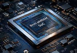
The rapid adoption of AI is accelerating demand for advanced packaging technologies, including higher-density redistribution layers (RDLs) and increasingly complex package architectures. In response, Asahi Kasei is expanding its technology portfolio to address evolving technical requirements across both liquid and film-based materials.
As semiconductor packages continue to increase in size and complexity, we are actively evaluating and developing solutions in both categories. Our objective is to provide customers with the flexibility to select the process technology that best aligns with their manufacturing requirements, whether that involves liquid-applied materials or film-based solutions.
Q. The newly developed PSPI film combines the strengths of liquid PSPI and dry film photoresist technologies. Could you share the strategic thinking behind integrating these two material platforms into a single solution?
The trend toward larger semiconductor packages is introducing new manufacturing challenges, particularly in process uniformity, material performance, and panel-level scalability. To address these issues, we work closely with customers to understand their specific requirements and develop optimized material solutions.
For panel-level packaging applications, lamination has emerged as an effective method for forming insulating layers across large-format substrates. We are therefore advancing both liquid and film-based technologies to support next-generation package designs while enabling efficient, high-quality manufacturing processes.
Q. As semiconductor packaging moves toward larger interposers, finer wiring patterns, and more complex 3D structures, what are the biggest technical challenges customers are currently facing, and how does the new PSPI film help address them?
Customer requirements vary significantly depending on package architecture, manufacturing flow, and production scale. As a result, we support both liquid and film-based process technologies to meet a broad range of application needs.
Our PSPI Film and SUNFORT™ product families are film-based solutions designed to simplify resin application through lamination processes. These materials offer distinct advantages in process efficiency and uniformity, particularly for larger substrates and advanced packaging applications. We are also collaborating with equipment manufacturers and industry partners to further expand the capabilities and adoption of film-based processing technologies.
Q. Asahi Kasei is developing solutions that integrate the PSPI film with both the SUNFORT™ TA and CX series. How important is ecosystem-level collaboration in accelerating adoption of next-generation advanced packaging technologies?
We maintain close communication with customers to identify emerging challenges and develop solutions that address evolving market requirements. While we cannot disclose specific development programs or future product plans, our focus remains on delivering innovative materials that support the continued advancement of semiconductor packaging technologies.
Q. AI infrastructure growth is driving demand for higher-density and more power-efficient semiconductor packaging. How is Asahi Kasei positioning its Electronic Materials business to support the evolving needs of AI data centres and advanced chipmakers globally?
Asahi Kasei is positioning its Electronic Materials business as a First Priority Business in our current management plan. The goal is to achieve long-term growth by leveraging our strengths in advanced semiconductor packaging and high-performance materials. Driven by expanding AI workloads and increasing demand for advanced packaging technologies, we expect strong growth in key products such as Pimel™ photosensitive insulating materials, while also enhancing the value proposition of our glass fabric technology.
Looking toward 2030, we are focused on strengthening our leadership in niche, high-functionality materials for advanced semiconductor and high-speed communication applications. The strategy centers on accelerating growth of flagship electronic materials brands, including Sunfort™ and our capsule-type latent curing agent Novacure™, while pursuing strategic partnerships, technology collaborations, and targeted M&A opportunities. By combining materials innovation with close engagement across the semiconductor value chain, we aim to capitalize on emerging opportunities in AI and advanced packaging by 2030.
Q. Looking ahead, what opportunities do you see for Japanese materials innovation in strengthening the global semiconductor supply chain, particularly in advanced packaging and panel-level manufacturing technologies?
Japan has a strong presence of semiconductor materials and equipment manufacturers, and we believe opportunities to contribute to the resilience and advancement of the global semiconductor supply chain will continue to expand.
By developing proprietary technologies that drive next-generation semiconductor innovation, we remain committed to fostering the growth of the global semiconductor industry while contributing to society.