Kyocera and Tohoku University Advance Optical Isolators for Silicon Photonics and CPO
21 September 2026 |
Interaction
Laser-annealing technology enables optical isolators to be integrated directly onto silicon photonics chips, supporting smaller, scalable architectures for AI datacentres and next-generation optical interconnects.
Semicon Leaders Asia speaks with Tomoya Sugita, Manager, Optical Research Section, Advanced Technology Research Institute, Kyocera Corporation, about Kyocera’s laser-annealing technology for monolithically integrated optical isolators and its potential to advance silicon photonics, CPO, and AI data centre interconnects.
Q. What industry and market requirements are driving the need for monolithically integrated optical isolators, particularly as silicon photonics and co-packaged optics (CPO) become increasingly important for AI data-centre infrastructure?
As AI training and inference workloads continue to scale, interconnect performance and power consumption are becoming major bottlenecks within data centres. To address this challenge, the industry is moving the point of optical-electrical conversion closer to the compute chip—from pluggable optical modules installed at the front panel of the equipment towards co-packaged optics (CPO), in which the optical components are placed adjacent to the compute chip. Ultimately, laser light sources themselves are expected to be integrated within the package and, eventually, directly onto silicon photonics chips.
As light sources are integrated closer to optical circuits, back-reflected light becomes an unavoidable issue. Optical circuits inevitably contain points of reflection, such as waveguide facets and fibre-coupling interfaces. If reflected light re-enters the laser, it can destabilise oscillation and increase noise. Moreover, as transmission speeds increase, modulation formats with smaller noise margins, including multilevel modulation, are being adopted. Consequently, the need to manage back-reflected light becomes more critical with each successive technology generation. As long as end-product performance requirements continue to rise, we expect optical isolators to remain essential for suppressing back-reflected light.
Conventional bulk optical isolators, however, cannot physically keep pace with this trend towards integration. These millimetre-scale free-space optical components require precise alignment and assembly on an individual basis. High-density packages such as CPO do not have sufficient space to accommodate them. In addition, as the number of lanes increases and each package incorporates many light sources, fitting a separate component to every lane becomes impractical in terms of size, cost and assembly workload. When lasers are integrated directly onto an optical circuit chip, they must also be protected from reflections occurring before the light leaves the chip. In that configuration, the only practical option is to incorporate the isolator into the waveguide—in other words, to build it directly into the optical circuit itself.
Q. Kyocera and Tohoku University use localised laser annealing to heat the magneto-optical garnet without exposing the rest of the silicon photonics chip to high temperatures. How does this approach overcome a key manufacturing barrier to integrating optical isolators directly onto photonic chips?
Magneto-optical garnet requires high-temperature heat treatment before it can function as an optical isolator. Heating the entire chip, however, risks damaging other devices and electrodes on the same chip. Aluminium, which is commonly used for electrodes, can be damaged at temperatures above 400°C and therefore cannot withstand the temperatures required to crystallise magneto-optical garnet. An alternative approach, in which material fabricated on a separate substrate is bonded to the chip, also presents mass-production challenges, including alignment accuracy and the number of individual mounting operations required.
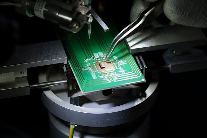
Our approach uses a laser to irradiate only the required region, crystallising the magneto-optical garnet without exposing the surrounding area to high temperatures. Microscopic observations confirmed that the electrode patterns on the same chip showed no peeling or melting. Because the process can selectively treat only the required areas, it is highly compatible with integration into conventional semiconductor manufacturing processes. In principle, it should also be possible to irradiate multiple points across a wafer. This approach therefore has the potential to overcome the limitations of conventional methods in terms of both mass manufacturability and device-design flexibility.
Q. The demonstrated device achieved a 13.6 dB isolation ratio and reduced back-reflected light by approximately 95%. How significant are these results for practical optical communication systems, and what performance improvements are still required for commercial applications?
The primary significance of this achievement is that, for the first time, magneto-optical garnet formed directly on a silicon photonics circuit was activated by laser annealing and demonstrated to operate as an optical isolator. In other words, we showed that a functional device can be produced using a process compatible with semiconductor manufacturing.
The demonstrated isolation ratio of 13.6 dB suppresses back-reflected light to approximately one-twentieth of its original level, representing a reduction of about 95%. This is an important proof-of-concept result. At the same time, other research groups have reported integrated optical isolators with isolation ratios roughly twice that achieved in this work. We therefore recognise that further improvements in the isolation ratio, together with lower insertion loss, will be required before the technology can be deployed in practical systems. We will address both areas in the next stages of development.
Q. How could integrating optical isolators directly onto silicon photonics chips benefit next-generation CPO architectures in terms of optical performance, system size, power efficiency and design flexibility?
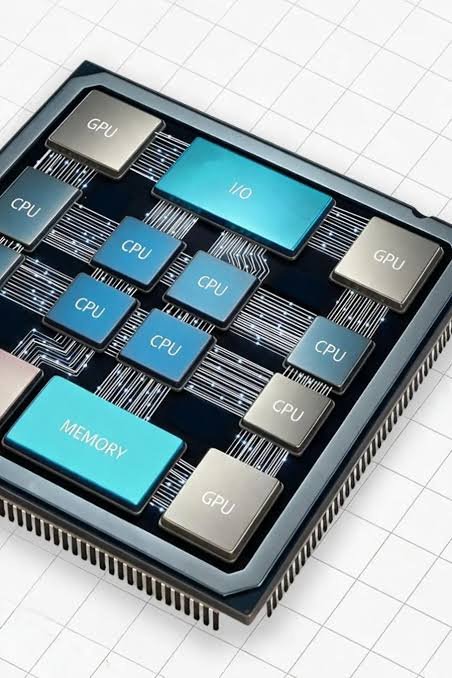
In CPO, semiconductor chips that perform computational processing and silicon photonics circuits are densely integrated within a single package. Conventionally, optical isolators have had to be mounted as separate components, creating constraints in terms of miniaturisation, component count and assembly workload.
The ability to fabricate optical isolators directly on an optical circuit is expected to offer three main benefits. First, reducing the number of components and assembly steps can enable smaller packages. Second, it can support configurations in which a laser source is integrated with the optical circuit and an isolator is positioned immediately after the source, helping to ensure stable laser operation. Third, designers will be able to place optical isolators at the required locations and in the required quantities within the circuit, providing greater design flexibility.
As next-generation CPO systems move towards more lanes and higher transmission speeds, laser stability will provide a foundation for both signal quality and power efficiency. The prototype developed in this study is a silicon photonics circuit incorporating an optical isolator; it is not yet a complete CPO device. Looking ahead, we envisage integrating the isolator on the same chip as other optical functions, such as optical modulators.
Q. What are the main manufacturing and scalability challenges that Kyocera and Tohoku University need to address before this laser-annealing technology can move from laboratory demonstration to high-volume production?
There are two principal challenges. The first is to improve the optical isolator's fundamental performance. This includes increasing the isolation ratio, reducing insertion loss and further reducing the device footprint.
The second is to optimise the process for mass production. Key requirements include reducing the irradiation time, which is currently approximately 30 minutes; optimising the irradiation conditions; ensuring uniformity and reproducibility across the entire wafer; increasing throughput through multi-point irradiation; and conducting detailed electrical evaluations of the impact on surrounding circuitry. Addressing these issues and developing a process that can be incorporated into standard semiconductor manufacturing flows will be critical to moving the technology from laboratory demonstration to high-volume production.
Q. Looking ahead, where do you see the strongest commercial opportunities for the technology, and how will the collaboration focus on reducing optical loss, improving efficiency and increasing manufacturing productivity to support the growing demand for silicon photonics?
We see the greatest commercial opportunity in optical interconnects for AI data centres, including silicon photonics optical transceivers and CPO. We expect the need for this technology to grow as the integration of laser light sources advances. Potential applications also extend to any field in which laser sources and optical circuits are expected to be integrated, including telecommunications, sensing, LiDAR and photonic quantum computing.
We have not yet determined the specific route to commercialisation. However, we are considering the most appropriate model for bringing the technology into practical use, including the possibility of technology licensing.
Through the joint research between Kyocera and Tohoku University, we plan to reduce optical loss and improve the isolation ratio through advances in both material quality and device design. We will also work to achieve smaller, more efficient devices by enhancing the properties of the magneto-optical material, while improving manufacturing productivity by shortening irradiation times and introducing multi-point irradiation.